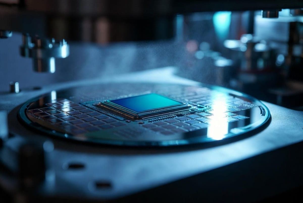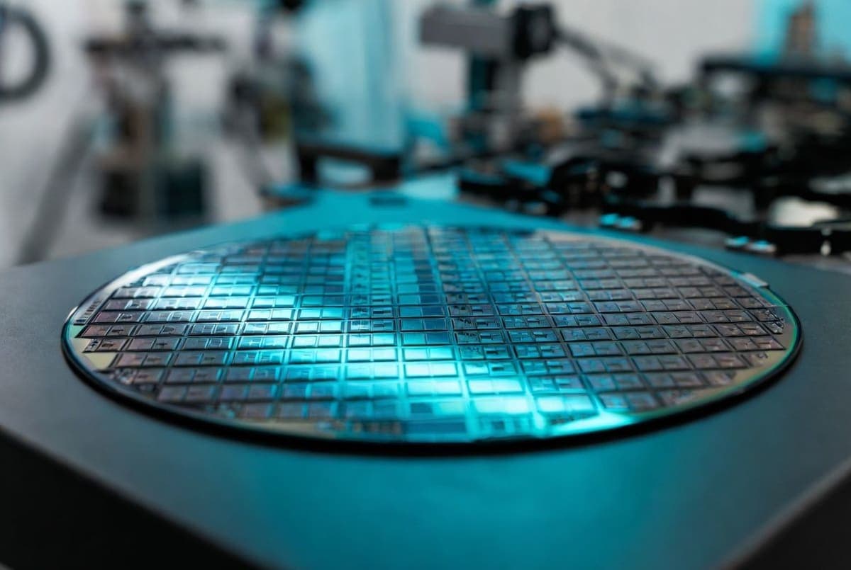
Engineers from Stanford, Carnegie Mellon, Penn, and MIT have manufactured what they claim is the first monolithic 3D integrated circuit produced at a commercial US foundry. SkyWater Technology fabricated the prototype at its 200mm production line in Bloomington, Minnesota, using a mature 90nm to 130nm process.
What "monolithic" actually means here
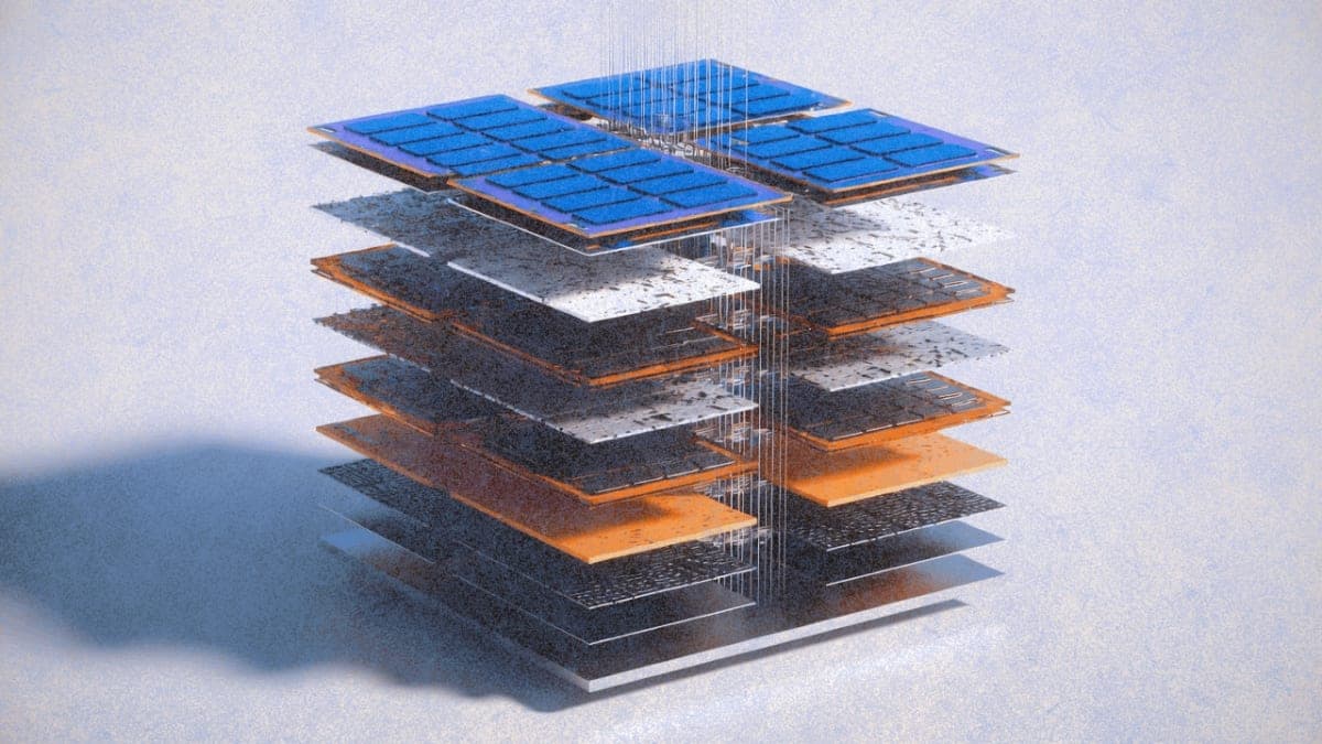
Previous 3D chip attempts mostly involved stacking separate, finished chips and bonding them together. The connections between layers tend to be rough and limited, which creates its own bottlenecks. This team did something different: they built each layer directly on top of the previous one in a single continuous process.
The trick was temperature. Building new layers typically risks destroying the circuitry already fabricated below. The researchers designed the entire process around a thermal budget of roughly 415°C, low enough to protect underlying layers while still allowing sequential fabrication.
The result is a stack that integrates conventional silicon CMOS logic with resistive RAM layers and carbon nanotube field-effect transistors. "It's like the Manhattan of computing," said Robert Radway from the University of Pennsylvania, and yes, researchers do love their skyscraper metaphors. But the analogy isn't entirely hollow: vertical wiring acts as high-speed elevators shuttling data between floors, and the whole point is density.
The numbers
Hardware testing showed roughly a fourfold improvement in throughput compared with equivalent 2D implementations at similar latency and footprint. That's a real measurement from a real chip, which matters because most 3D integration claims come from simulations alone.
Simulations of taller stacks, with additional tiers of memory and compute, showed up to twelvefold improvements on AI workloads derived from Meta's LLaMA model. The team projects that the architecture could eventually deliver 100- to 1,000-fold improvements in energy-delay product, a combined metric of speed and efficiency. Those projections should be treated with appropriate skepticism: simulated performance rarely translates directly to production, and the gap between lab prototypes and commercial chips is where many promising architectures go to die.
Why this timing matters
The AI industry has spent much of 2025 confronting a problem engineers call the "memory wall." Large language models like GPT and Claude constantly shuttle enormous volumes of data between memory and computing units. On conventional 2D chips, everything sits on one flat surface, forcing data through a small number of long, crowded paths. The computing parts run faster than data can be delivered, so the system ends up waiting.
For decades, chipmakers addressed this by shrinking transistors and packing more onto each chip. That approach is now hitting physical limits. Memory chip prices have doubled or tripled in some segments this year as companies prioritize high-bandwidth memory for AI servers over conventional DRAM for phones and laptops. SK Hynix has reportedly told analysts that the memory deficit will persist through late 2027.
Building upward rather than outward offers one potential escape route. Whether this particular architecture scales to production remains an open question.
The domestic manufacturing angle
The paper was presented at the 71st Annual IEEE International Electron Devices Meeting in San Francisco earlier this month. Beyond the technical claims, the team emphasized that the entire process happened at a US foundry.
Mark Nelson, SkyWater's vice president of technology development, described the effort as proof that monolithic 3D architectures can transition from university cleanrooms into domestic manufacturing. Given ongoing concerns about semiconductor supply chains and the billions in CHIPS Act funding flowing into US fab capacity, the timing of that message is not accidental.
The research received support from DARPA, the National Science Foundation, Samsung, the Stanford Precourt Institute for Energy, the Stanford SystemX Alliance, and the Department of Energy, among others. The work was conducted across Stanford, CMU, Penn, and MIT.
Subhasish Mitra, the Stanford professor leading the project, put the stakes bluntly: future AI systems will demand 1,000-fold hardware performance improvements. Whether monolithic 3D integration delivers on that promise, or joins the long list of promising architectures that never made it to volume production, is a question that won't be answered for years.