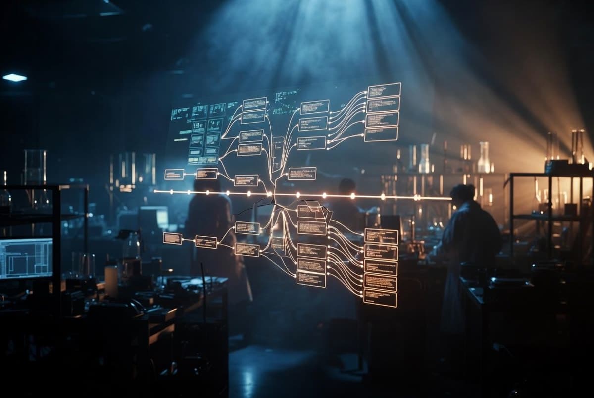
On Monday, May 25, at the IEEE International Symposium on Circuits and Systems in Shanghai, Huawei semiconductor chief He Tingbo proposed scrapping the metric the chip industry has lived by for half a century. Her keynote, "New Semiconductor Path in Practice," introduced what Huawei calls the Tau Scaling Law, a way of measuring chip progress that has nothing to do with how small you can make a transistor.
Moore's Law counts transistors per square millimeter. Tau counts time. Specifically the time a signal needs to cross a wire, which He's team defines as the product of resistance and capacitance: the RC delay. Shorten the wire and resistance, capacitance, and delay all drop together. That's the pitch.
Why now
The old game stopped paying off somewhere around seven nanometers. You can still shrink the transistor, but the wires between transistors now dominate the delay, and lithography has run into the wavelength of light itself. Then there's the bill. An EUV machine runs north of $150 million, and designing a 2nm chip has crossed the billion-dollar line. Cost per transistor, which fell reliably for fifty years, has stopped falling.
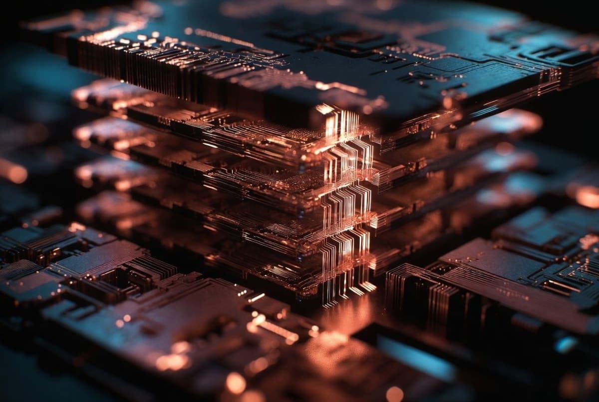
Huawei's answer is architectural, not lithographic. Its LogicFolding design stacks chip logic vertically instead of spreading it across a plane, which collapses the distance a signal travels. On the Kirin chip due this autumn, Huawei says that pushed transistor density up 55 percent without changing the manufacturing process, jumping from 155 to 238 million transistors per square millimeter in one step. He claims the same gain would have taken three years and two process nodes the old way. Worth remembering Huawei has spent six years quietly mass-producing 381 chips on this principle, so this isn't a paper concept.
The branding problem
Not everyone is buying the framing. The Register's headline put it bluntly, calling the announcement more marketing than breakthrough, and the skepticism isn't unreasonable. Stacking transistors into layers is something Intel and TSMC have researched too, so the underlying idea isn't Huawei's alone. What's new is the name attached to it. Huawei's own colleagues have reportedly started calling it "Her's Law," which tells you something about how much of this is positioning.
A few things deserve caution. The "1.4nm by 2031" target is density equivalence, not an actual 1.4nm transistor, and equivalence is not parity. Nobody outside Huawei has seen the thermal data, the design tools, or the software story. And it's one chip line, not an independently verified platform.
What this is really about
The chip is almost beside the point. Washington built its entire export-control strategy around denying China access to EUV machines. A path that doesn't need the newest EUV tools breaks the main lever.
You can see the same logic that played out with DeepSeek and Qwen. Once advanced computing gets cheap and plentiful, the scarcity that props up Nvidia's margins starts to evaporate. Jensen Huang already conceded the point. In a CNBC interview on May 21, he said Nvidia has largely conceded China's AI chip market to Huawei, describing his own company as having "evacuated that market," which is a generous way to describe being pushed out by sanctions.
The macro read is uncomfortable for anyone who assumed export controls would simply slow China down. Cut off the technology and China hunts for another route, and the engineering bench is deep enough to occasionally find one. So long as the work keeps getting published, the competition benefits everyone.
The test comes this fall. Huawei either shows the claimed numbers on shipping Kirin silicon, or the Tau Scaling Law stays a well-produced conference talk.