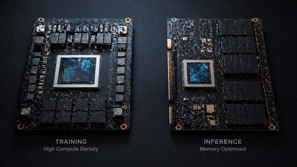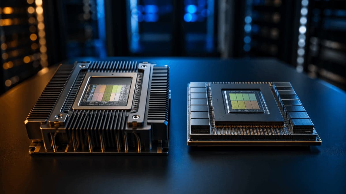
Google used its Cloud Next 2026 keynote on Wednesday to unveil the eighth generation of its Tensor Processing Unit, and for the first time, it is shipping as two chips instead of one. TPU 8t is built for training. TPU 8i is built for inference and reasoning. Both are coming "later this year," according to Amin Vahdat, Google's SVP and chief technologist for AI and infrastructure, who announced the chips.
This is the strategic bet. Nvidia sells one chip family and lets the software sort workloads out. Google is doing the opposite: specialized silicon for specialized jobs, with the obvious trade-off that you're now committing to predictions about what AI workloads look like eighteen months from now.
What's actually different
TPU 8t is the big-iron training chip. A single superpod scales to 9,600 chips, holds two petabytes of shared high-bandwidth memory, and delivers 121 exaflops of compute. That is close to three times the per-pod compute of last year's Ironwood, which topped out at 42.5 exaflops across 9,216 chips. The technical deep dive adds that this generation introduces native FP4, a dedicated SparseCore for embedding lookups, and a claimed goodput target above 97%. Whether that goodput number survives contact with real million-chip training runs is a separate question.
TPU 8i is the more interesting design. It carries 288 GB of HBM and 384 MB of on-chip SRAM (three times more SRAM than Ironwood), which matters because reasoning models spend a lot of time moving key-value cache data around. Google also scrapped the familiar 3D torus topology used on the training chip. In its place: Boardfly, a flatter, high-radix design inspired by Dragonfly research. The claimed payoff is a 56% reduction in network diameter, which Google says cuts worst-case chip-to-chip hops from sixteen down to seven in a 1,024-chip pod.
And there is a new Collectives Acceleration Engine that Google says reduces on-chip collective latency by 5x. I'd want to see independent numbers on that before getting excited.
About those numbers
Google claims up to 2.7x performance-per-dollar on training and up to 80% better performance-per-dollar on inference compared to Ironwood. Two things to keep in mind. First, "up to" is doing heavy lifting in both figures. The 80% inference claim is qualified in the technical post as applying "particularly at low-latency targets for large MoE models." That is a specific workload shape, not a general claim.
But the bigger caveat is that every comparison is against Google's own previous generation. None of it is against Nvidia's current Blackwell or the Vera Rubin systems due out later this year. That isn't necessarily a criticism; it's just the shape of the announcement. Google doesn't sell TPUs as rack-level parts you can benchmark against an H200, and cross-vendor comparisons in this space are famously contested anyway. If you want something other than Google Cloud's marketing to evaluate the chips on, you're going to wait.
Who's actually buying these?
Anthropic, mostly. In early April, the company announced a deal with Google and Broadcom for multiple gigawatts of next-generation TPU capacity starting in 2027, reported elsewhere as roughly 3.5 gigawatts. That is on top of the one-gigawatt commitment from last October. The anchor customer for the chips Google just revealed is, effectively, the company training Claude.
Citadel Securities got the obligatory customer quote in the keynote. Anthropic's signature on the capacity contract is what actually matters.
One detail the keynote glosses: TPU 8t is reportedly designed by Broadcom, TPU 8i by MediaTek. Google has been spreading its custom silicon across design partners for a few years. "Google's TPU" is less vertically integrated than the positioning implies.
The agentic framing
The whole announcement sits inside "agentic era" language. Vahdat argues that agent workloads, with their long context windows, iterative tool use, and multi-step reasoning, put fundamentally different demands on infrastructure than traditional training or one-shot inference. Splitting 8t from 8i is Google's bet on that thesis being correct.
Maybe it is. The premise at least has the virtue of being testable. If reasoning models keep scaling the way they have in the past year, specialized inference silicon with more SRAM and tighter collectives could look prescient. If they don't, Google has split its roadmap for a workload shape that never fully materialized.
General availability is slated for the second half of 2026. Anthropic's larger 3.5 GW deployment is scheduled for 2027.